If you read no further, here is the summary: Ignore drill back off errors.
Here is an explanation of what drill back off is, and why just about anyone can ignore warnings about it, today.
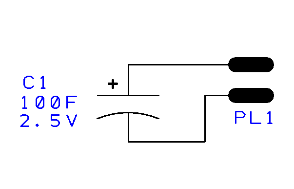
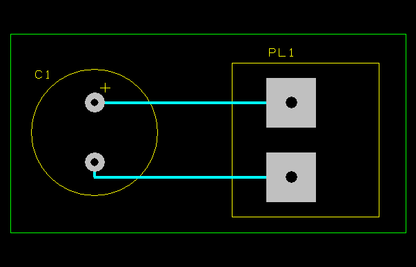
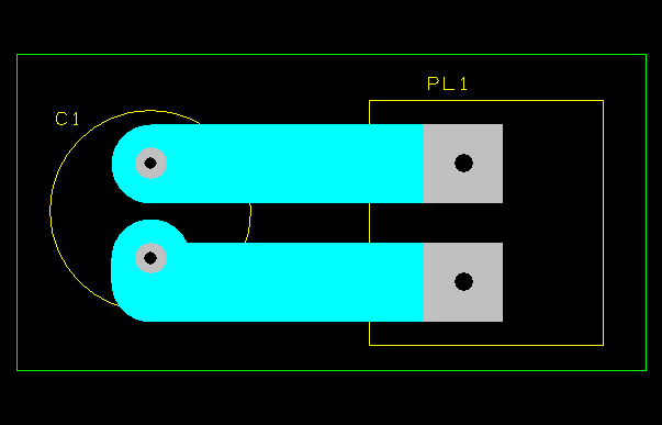
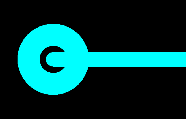
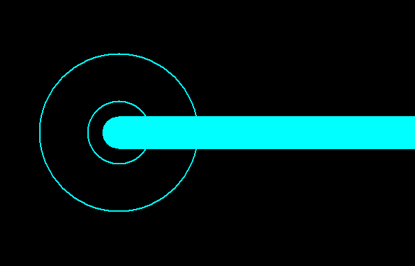
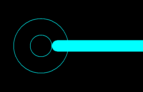
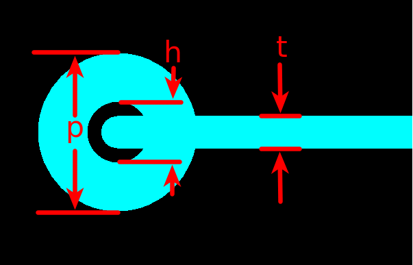
Here is a simple schematic, just a capacitor, and a connector.If you had your software automatically route a PC board, it might look something like this. The pads for the capacitor are 100 mils in diameter, and the traces are 10 mils wide. What doesn’t show is that the traces actually have rounded ends, and extend all the way into the exact center of the pad.Let’s say we were dissatisfied with the narrow traces of the previous layout, and decided to widen the traces to 250 mils, to carry more current. In looking at the trace to the top pad of the capacitor, we can now see that the trace actually goes all the way to the center of that pad, and has a radius about that point.Layout software often won’t show copper in a hole, under the assumption that the hole will be drilled out, anyway. This is what the copper layer around the upper pad of the capacitor will really look like if the design is fabricated as-is, but not drilled.The pad is shown as an outline here, for greater clarity. In the old days, when a human operator might be manually drilling the holes, there might be need for a clear target for the drill. In this case, and operator could still make out where the center of the hole is, but in the case where the trace was actually wider than the hole, there would be no target at all.Here is what some brilliant production engineer might do. They might “back off” the trace in the direction from which it came in, just enough to clear the hole and leave a perfect target for the drill operator. In fact, they could run a script on the entire design to back off all traces automatically for drilling.Here is the same pad as above, with a super-wide trace going to it. The trace is actually larger than the pad, and covers it completely.The trace has to be backed off quite a bit to clear the hole.Part of the radius of the trace is shown in outline to better illustrate what is going on. The trace is backed off so far, that the end point does not even lie within the pad. In fact, if the trace was short (like the one on the lower pad of the capacitor), the back-off could create a zero or negative-length trace (that is, a trace in the other direction). A trace in the other direction is very bad, as it could unintentionally short some other components.In packages like DesignSpark, in mathematical terms, a drill backoff error is generated when t > (p – h)/2, that is, when the trace is wider than the annular ring of the pad.
The reason we need not worry about this error today is that no contract manufacturer is going to alter the layout by backing off traces in such a manner. As the drilling is done by an NC (Numerically Controlled) robot drill, there is no need for a visible target. In fact, the drilling will typically be done on the board blank before any copper patterning even takes place.
Why this design rule check is still available in packages like DesignSpark is unclear to me, but fortunately, the check is optional, and can be turned off by unchecking a box. Most other layout software doesn’t even have the check at all.