
I bought a cell phone over the internet. When it came, I plugged in the charger, and nothing happened. The cell phone didn’t react, and the LED on the charger didn’t light, either. By substituting another charger, I determined that the phone was not at fault. Okay, dead charger. Now what?
That was the point where most normal people would say screw it, it’s not worth sending the bad charger all the way back to China for replacement. And the rational thing, even for an engineer, would have been to simply pick up another charger for a dollar at the local flea market. But I love a good debugging sleuth, so will look into it. [As of this writing — December 24, 2012 — I still don’t know what the problem is.] So I opened the charger up.

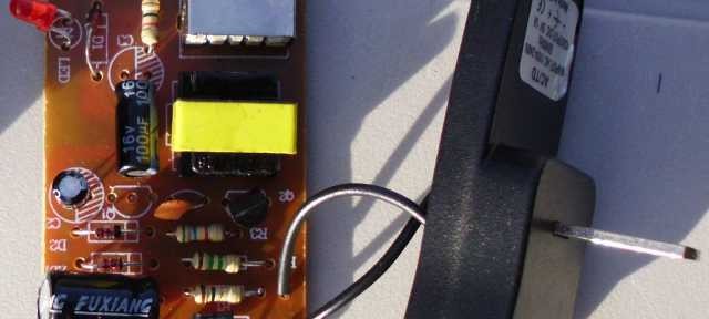
The first thing I noticed about the design was how simple it was. There wasn’t even an integrated circuit. I looked for burned components, loose connections, corrosion, and cold solder joints. In other words, my standard cursory check when looking at a circuit that I don’t understand. Looked all right.
The component count on the board was low enough that I could test each component individually. Again, without any understanding of the circuit. My only test equipment was a $5 digital multimeter, but even that can do wonders. Checked all resistor values. Seemed ok. Checked electrolytic capacitors. Yes, resistance that rises to infinity on the ohmmeter. One small-value capacitor – couldn’t check it. Checked transformer windings. There seemed to be three windings. Presumed to be ok since there was continuity. Checked diodes. Yes, they conduct in one direction only. I couldn’t check the avalanche voltage of the Zener diode, but that was secondary. There had to be a switching transistor somewhere, and Q2 was the only candidate. It read like two diodes both pointed away from one terminal. Presumed to be an NPN transistor, and ok. I was actually not expecting a bipolar transistor, because I was accustomed to designs where efficiency mattered, and FET’s were used. I was not accustomed to design for sheer cost. No money was wasted on full wave rectifiers in this circuit.
All right, looked like I would need to have some understanding of the circuit. As with any reverse engineering, the schematic below is just a guess.

Usually, most things that we fix worked at one time; that is, something broke. In this case, I couldn’t make that assumption. It could have been a manufacturing issue – a component missing, loaded backwards, or of incorrect value. Notice that Q1 is not loaded on the board? That was suspicious, but when looking at the actual circuit, I realized that Q1 is not actually connected to anything.
[December 28, 2012]
I wish I had an oscilloscope, but since I didn’t, I measured some voltages in the circuit. When the supply was plugged in C1 had 170 volts DC on it. C3 had zero volts. I have a working theory as to what’s wrong. Which of the following approaches would you take?
- Unsolder each component and test it individually
- Stare at the circuit and try to understand the theory of operation
- Try to find another similar supply, open it up, and learn from it
- Measure other voltages in the circuit
The next installment of this debugging story is here.