If you missed the introduction to this problem, it’s here.
[8:35 pm January 4, 2013] Okay, I’m back to this one. Here is the schematic again for reference.

My first theory was that R2 (1.5 MΩ) was too large. Perhaps it was erroneously loaded, instead of a smaller value. My reasoning was that if the rectified high voltage was about 150 volts, then the current into the base of Q2 would be about 100 uA. If Q2, which was unknown, had a current gain of 100, then that would mean 10 mA through the collector, and even if the entire 10 mA was drawn by the primary of T1, that would be 1.5 watts. But the output rating of the supply is 5 volts @ 1 amp, or 5 watts. Also, in looking at the voltage divider between R2 and R3 at startup, we would have a maximum of 0.55 volts at the base of Q2 at initial startup, not enough to drive it into saturation.
Since I didn’t have an oscilloscope, I decided to open up a similar cheap supply to see if my supposition was reasonable. To my surprise, the other supply had 10 MΩ to the base of its transistor! This brought me back to one of the basic principles of debugging: When you see hoof prints, think horses, not zebras. In other words, I should look for the simple and common, not the esoteric. And another debugging principle is known as the Eureka Principle: When you find the true root cause, you just know. On resistor R2, I was not sure, which was why I looked at another supply for guidance. When I have a “kinda, could be, maybe think so” feeling about a theory, then it’s usually not right.
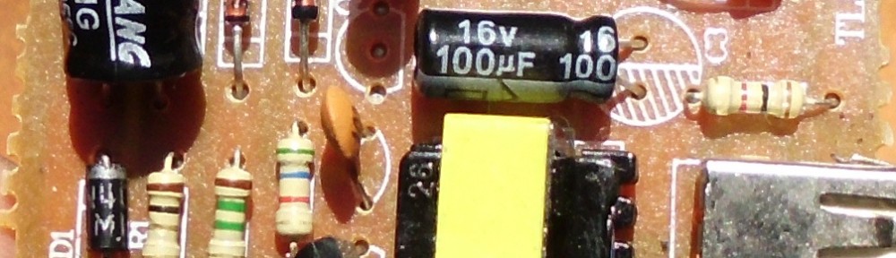
Here is my present thinking, which satisfies the Eureka principle. It would not have been possible to arrive at this theory from the information I’ve supplied so far on this blog. So here is a shot of the top of the board, and the bottom. The bottom picture has been flipped left to right, so that it matches the top in orientation.


During the reverse-engineering of this circuit, I didn’t know which leads of Q2 were emitter, base, and collector, so just connected them to a circle at first, then assigned them by looking at the circuit. That is the schematic that is shown above. However, when looking at the similar working supply, I noticed an xw-13001 transistor being used as the switch, and was able to find a datasheet for it. 400V NPN transistor, gain of 100, but the pins go B-C-E when read left to right on the front, not E-C-B. I looked again at the transistor on my failed assembly. It had “13001” stamped on it, and was probably the same thing. But still, it was inserted in an orientation that matched the silkscreen.
Here is what I will do. I will unsolder the Q2 from the board, and see if it is really B-C-E on my DVM, which has transistor sockets on it.
[10:14 pm January 4, 2013] All right, I unsoldered the transistor and tested it. In fact, the pinout does seem to be E-C-B. However, the transistor showed a gain of 1 on the tester. I tried another transistor from my parts box to verify that the tester was okay. Yes, gain of 308 on the known good transistor. So my theory now is that it was a bad transistor.
[9:12 pm January 5, 2013] I unsoldered the XW13001 from the similar supply. In fact, that transistor has the B-C-E pinout on the data sheet. And the DVM shows a gain of 18. That seems low, but maybe that’s how it is with high voltage transistors. Wait, maybe it’s B-E-C, and I was measuring the reverse transistor. Let me check.
[11:05 am January 7, 2013] It turned out to be too difficult to bend the leads to test whether the pinout on the XW 13001 was actually B-E-C, but I would think that the datasheet would be accurate. This type is supposed to have a gain from 40 – 80, so at least it had something. I soldered it into the circuit, and energized. Nothing. No output voltage, and voltage across C2 basically zero. I think this oscillator is basically not starting at all. I’m pretty sure that the transistor I removed was bad, with a gain of 1. And a third principle of debugging comes into play here: Usually, only one thing is broken (unless the original failure led to a cascade of other failures). I was starting to doubt whether the R2-R3 combination was right, whether that was preventing the oscillator from starting, but what are the chances of having a bad transistor AND loading an incorrect value of resistor(s)? Quite low. Unless, this was a cascade failure. Could having too little bias on the base of Q2 have led to its failure originally? I think not, but I will unsolder the replacement transistor to see if it now has burned out and has a gain of 1. If not, then maybe a gain of 18 is simply not enough, and I need to find another transistor to try.
[5:18 pm January 13, 2013] Tried changing R3 to 82k, and replacing the transistor. It still doesn’t produce 5 volts, although I do see something like 14 mV at the output. That’s interesting, because it is not zero. The output capacitor rapidly decays to zero volts when left alone, so that must mean that there’s at least a little oscillation going on. My friend Phil recommended checking the Zener. I thought that couldn’t be it, since it read ok as a diode, but now I think I’ll unsolder it and actually check the avalanche voltage.
[2:47 pm January 14, 2013] I was able to test the zener in-circuit (but not powered). It’s 6.75 volts, which seems reasonable enough. I should try measuring the voltage across the zener when the circuit is powered. This blog jumps in time, as I only get back to this project occasionally.
[10:16 am January 17, 2013] I measured the voltage across C2 with the power turned on. -2.7 volts. Repeat, negative 2.7 volts, i.e., the capacitor is reverse-biased. WTF?? I had changed Q2 to a brand new transistor, and changed R3 to 82k. What should I measure next?
[2:16 pm January 17, 2013] What could possibly have reverse-charged C2? There’s no path to it, not without going the wrong way through a diode. And even if there was a path for charging, the base of Q2 should be clamping the voltage to 0.6 or 0.7 volts max. With the power turned off, I checked Q2. It’s OPEN CIRCUIT now. I burned it out. And Zener ZD1 is now a dead short. Looks like that burned out, too. I remember Q2 feeling hot when I first energized the circuit. My theory is that it went into thermal runaway, and dumped a ton of current into the zener, burning it out, too. I know that the zener wasn’t always bad – I had just tested it a few days ago. Other duties call – I’ll return to this sleuth later.
The conclusion of the saga is here.