Q2, a MOSFET acting as a synchronous rectifier, had burned out in a previous experiment. I put a scope on the gate to see what was going on.
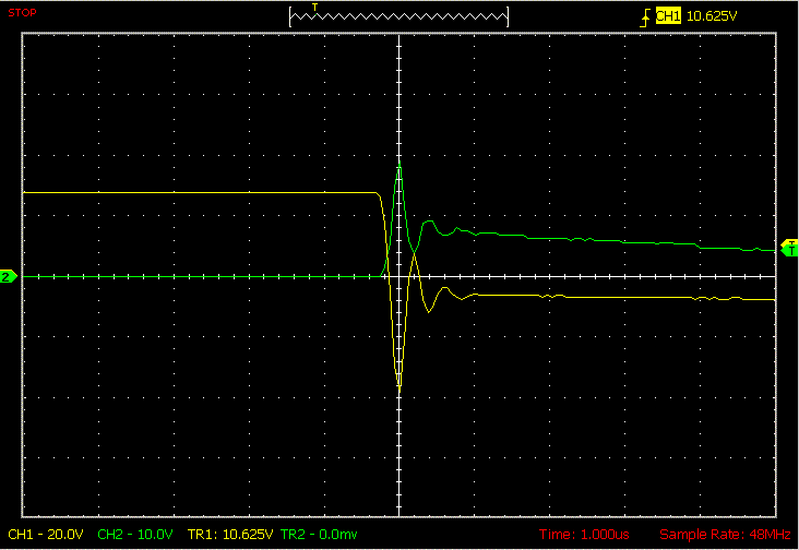
The interval during which channel 1 (yellow) is +24 volts is when Q3 is on. When Q3 turns off, the signal goes negative relative to scope ground, as energy is transferred to the output. At the same time, the gate drive (channel 2, green) turns on. As there is considerable ringing in the circuit, the gate drive spikes to almost 20 volts initially – the maximum allowable voltage on the Q2 gate. Before the gate winding was reduced from 4 turns to 3, this spike would have theoretically reached about 27 volts. That is probably what destroyed the original Q2 after a few minutes of operation.
Even with the gate winding at 3 turns, there is too little margin for this engineer’s comfort. If the output voltage was higher, the gate drive on Q2 would again exceed the 20 volt spec. I’m beginning to realize why we don’t see self-timed synchronous rectification with inverting converters.
- The design is very sensitive to selection of analog components. If the gate is not driven hard enough, no synchronous rectification goes on.
- If the gate is driven too hard, when the converter goes into discontinuous operation, massive amounts of energy are lost as the output discharges into the input.
- The cutoff of the gate drive is dependent on an RC decay, so will never be as efficient as a rectangular pulse with optimum timing.
I think I’m going to go to a digitally-timed gate drive. To do the level translation, I will need a pulse transformer winding for every gate (there are 12 in the actual design).
But the real reason I demurred or a digital solution was the PICAXE. Using PICAXE BASIC, it is not possible to generate the timing pulse for Q3, and also a pulse with the right phase and duration for Q2. The actual PIC is capable of such output, but that would force me into abandoning BASIC and (possibly) in-circuit programming, too.