If you’re joining this thread in the middle, you probably want to read the beginning first.
[9:28 pm January 18, 2013] Root cause at last! Here’s the schematic for the last time, with some annotations:


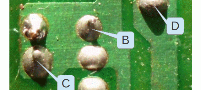
I had measured between A and D and read a fraction of an ohm, which is how I concluded that the winding of the transformer was good. But then, I measured between A and B, and there was no connection. I checked B and C, those were connected just fine. Went back to A and C. No connection! The picture above was taken before rework – can you see any cold solder joint, or cracked printed circuit trace? Neither could I, but meters don’t lie.
An open connection at A was consistent with the failure seen, burnout of Q2 and ZD1. Thank goodness we have a local electronic store, Halted Electronics, that still sells individual parts. The replacement KSP45 transistor was 35¢, and 1N754 Zener diode was 14¢. In any other place in the world, I’d probably have to resort to eBay to get parts.
After resoldering the cold joint, I energized the circuit, and saw the LED light for the first time ever. Success!
This quest made me wonder whether I should add another debugging rule. I was looking for incorrect parts, or mis-inserted parts. In this day of automated assembly and parts flows, such a mistake is increasingly unlikely, and even if it did happen, it would probably affect an entire lot of devices, and be seen immediately. The failure I saw was one of workmanship (a cold solder joint), and made me think that this should be the number one consideration for cause of a device that doesn’t work out of the box.
It also suggested to me that cheap devices like this phone charger are never tested by the manufacturer, or perhaps tested only on a sampling basis. I find it implausible that this device once worked, then went bad later. The only way to get the cost down is to have a process so reliable, that the vast majority of devices work. I’m guessing it’s cheaper for the manufacturer to just deal with occasional duds than to test every unit.
please what’s the function of C2 in this circuit and why are the pins oriented as such?
Good question. My guess is that the bias at the base of the transistor needs to be a steady voltage, and C2 serves to average the high frequency spikes coming from the feedback winding of the transformer. Since the voltage at the anode of the zener is negative, C2 is oriented to filter this negative voltage appropriately.
But that’s just a guess; this is not my design.
Thanks a lot
My thinking for C2 is to provide a negative supply (with respect to ground). Some other cheap supply schematics seem to carry this signature design. In one power supply that I have dissected, there is a quench circuit that is driven by voltage that will stop the oscillation (via an optocoupler), presumably when the output voltage is sufficient (a form of voltage regulation). I will put the schematic in my blog: ketutstechblog
The optocoupler sounds like a clever way to get analog (not just on/off) feedback on the output voltage, and probably more accurate, too. In the inexpensive design above, the extra transformer winding is acting as a proxy for the output voltage. Safety regulations prohibit an actual current path between the line and output, as we know.