I need an inductor of a certain value for my solar bike. Unfortunately, working with scavenged and surplus parts, it’s hard to get the value I really want. It would be easy to measure an inductor with an LCR meter, or with a simple circuit plus an oscilloscope. I have neither, so have to be creative about it. (Kind of reminds me of high school, when I had only a multimeter, so measured capacitance by building an oscillator and listening to the tone through headphones…)
A PICAXE-08M2 embedded processor is the heart of the circuit above. That processor has built-in A/D converters and pulse generators. Here is pseudo-code for its program:
set_low(peak_detector_capacitor); // zero out to start
set_to_input(peak_detector_capacitor);

voltage = 0;
count = 0;
// Pulse the power transistor
// Peak current across sense resistor is translated
// to voltage, and picked up by peak detector
// It may take several pulses to charge the capacitor
// in the peak detector, so keep pulsing until the
// reading is stable
do {
    last_voltage = voltage;
    pulse(gate_of_mosfet);
    voltage = readadc(peak_detector_capacitor);
    count++;
    } until ((voltage - last_voltage) <= 1);
print("The voltage is ", voltage);
print("Number of iterations ", count);
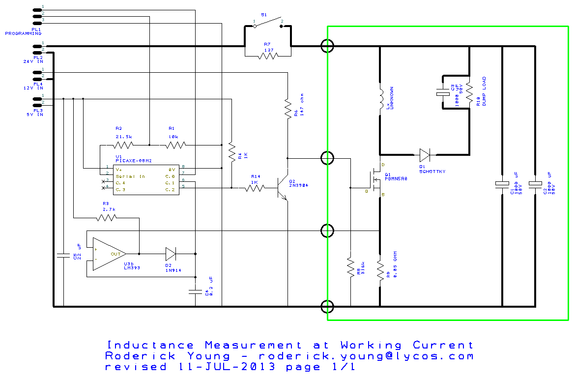
Here’s how it works:
- There are several power supplies, but the 24-volt supply comes from lead-acid batteries.
- C1 and C2 are stiffening capacitors, since there will be transient currents of perhaps 40 amps on 24 volts.
- S1 enables power on 24 volts. R7 is there to gracefully charge C1 and C2 upon initial connection to the batteries. Without R7, there will be a big spark when the leads are initially connected, or when the switch is first turned on.
- U1 is the aforementioned PICAXE processor, with R1 and R2 as standard interface components to the programming port, a 3-wire serial interface. Output from the program is sent through this same port to a terminal.
- Lx is the unknown inductor to be measured. When Q1 is turned on, roughly 24 volts is applied across the inductor. Current builds up in the inductor according to the equation V = L di/dt. Thus, if we know the duration for which the voltage is applied (dt), and the peak current (di), we should be able to calculate the inductance.
- The current flowing through the inductor also flows through sense resistor R9. As it does, a voltage develops across R9. This voltage is large enough to be measured, but small enough so as not to significantly interfere with the current through the inductor.
- U3, D2, and C4 form a peak detector circuit that monitors the voltage across R9. U3, an LM393, has an open collector output, so needs pullup R3. In order to get better precision, R3 has a higher value than would be capable of charging C4 to its final value within the time of one pulse, so it is necessary to pulse current through Lx multiple times.
- U3 is a bipolar part that has significant input bias current, so will charge C4 on its own if left alone. An FET input comparator would have lower drift, but as implemented, the voltage on C4 can be read quickly before significant drift occurs.
- Pin 5 (C.2) on the PICAXE is a low-true signal to drive a pulse to the gate of Q1. The 5-volt output of the PICAXE may not be enough to turn on Q1 solidly, so Q2 and R6 are used to invert and level-shift the signal to 12 volts.
- When the PICAXE is going through initialization or programming, and its pins will float. R4 insures that Q2 is turned on at this time, and in turn, that Q1 is turned off.
- R8 insures that static does not build up on the gate of Q1 and harm the transistor when the breadboard part of the circuit (outside the green box) is disconnected
- When current is flowing through Lx, and Q1 turns off at the end of a pulse, voltage builds across Lx, possibly to levels that would destroy Q1 if left unchecked. Therefore, R10 is used as a dump load to absorb the excess energy. The initial pulse of current through R10 would be quite high, and result in a high voltage, except that C3 absorbs the bulk of the current spike. R10 is actually a 12-volt automotive lamp, so that if Q1 is pulsed continuously, there should be a visual indication of the power output.
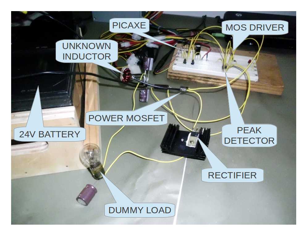
And here is what it looks like in real life:
[18-JUL-2013] I don’t fully understand the results I got. Perhaps you, the reader, can help. The original drive circuit is shown below for reference.
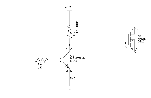
At first, I used a resistor of 1000 ohms for R1, and got a reading of 14.4 amps. Theoretically, it should have been 24 amps, with a perfect switch, and a perfect inductor. Possibly the gate of the MOSFET Q1 was taking too long to charge? So I changed R1 to 261 ohms, and got 19.4 amps. Good, right direction. Then I dropped R1 to 137 ohms, and got 21.4 amps – close enough, given all the unknown tolerances in the circuit. So it looked like I needed to do some work on the gate drive.
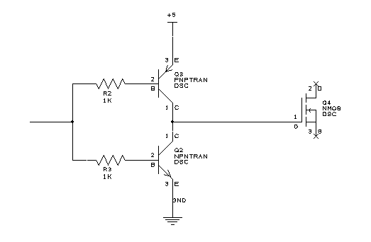
The totem-pole drive above was my next attempt. This is similar to a TTL output, and should have a very low impedance both for charging and discharging the gate. Also, this configuration uses less power than the RTL drive above, since the NPN transistor does not need to sink any static current for the low state. With this circuit, I got a reading of 21.6 amps. Note that the supply voltage is only 5 volts here, but this seems to be all right, as the power MOSFET is designed for a logic level drive, with a low threshold voltage. A weakness of this circuit is that at startup, the driving processor pin is floating, so current flows out of the base of the PNP transistor, through the two base resistors, and into the base of the NPN transistor. Both transistors are turned on simultaneously, for a temporarily high power dissipation. If I actually end up using a totem pole, I will probably use NMOS and PMOS FETs, which will have less of this problem.
Just for the heck of it, I decided to try driving the power MOSFET gate directly from a processor pin. I had low expectations.
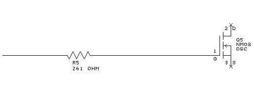
Surprisingly, with the MOSFET gate connected directly to the processor pin (R5 = 0 ohms), I measured a peak current of 21.8 amps. I put in 137 ohms, expecting the result to be smaller, but then saw 25.8 amps. That didn’t make sense to me. I increased the resistor to 261 ohms, and got 26.3 amps as the peak current. Finally, I tried 1000 ohms, and got nothing. Perhaps there was not enough time to charge the MOSFET gate to turn on in the 10 uS pulse I was using? For that matter, with the lower value resistors, perhaps the gate was never fully turning off?
With bolstered confidence, I put the 261 ohm resistor back into the circuit, and altered the software to put out a continuous train of pulses at increasing duty cycles. I connected a voltmeter across the dummy load, but was disappointed to see just 0.1 volt there when the duty cycle was cranked up to about 33%. If my calculations were correct, at that point, the lamp in the dummy load should have been at full brightness. I had not heat-sinked the transistor, thinking that these first few experiments would be at low power. Then, POP! The power MOSFET had gotten so hot, it unsoldered itself, and as the wire sprung away, there was a blue spark. Well, at least that confirmed that high currents were present.
So what happened? Anyone?? I think I’ll have to break down and buy an inexpensive USB oscilloscope. This would be so much easier to debug if I could see what’s going on.
[23-AUG-2013] Update: I bought an oscilloscope, which made finding root cause of this issue easy. Read about it here.