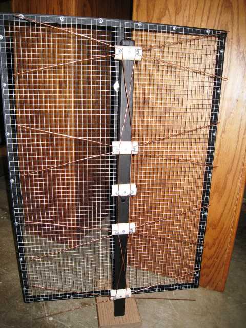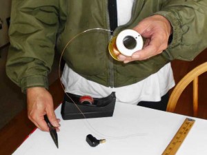
Since the early 80’s, I have had cable or satellite TV, both as a single person, and later when we got married. That is, until about 2009. The employment situation at work was unstable, and as a proactive measure to save costs, we were going to switch satellite providers. We got Direct disconnected, and decided to delay getting Dish for a little while to save a few extra dollars. But we discovered that we really didn’t miss premium TV much, especially since we could receive about 80 free digital broadcast channels.
The only problem was that the TV antenna needed to be positioned a certain way to get one channel, then repositioned to get another. It was an issue that I hadn’t had to deal with for 30 years.
My friend had built his own 4-bay bowtie antenna and had great results, so I decided to try, the goal being to have an indoor antenna that did not need to be repositioned. Here are the plans that he used: element layout and 4 bay phase lines .

For my prototype, I went against the design specification of 1/8″ diameter wire, and used cheap #28 magnet wire. Instead of a sturdy frame, I just taped the antenna to a scrap piece of cardboard. I soldered the connections between the elements and the phase lines. And I skipped the reflector.


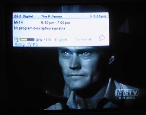
Here is the reception of some selected channels with the store-bought antenna in its best position:


And here is the reception of the first prototype DIY antenna:
Note that the home built antenna appears to have higher gain than the store-bought one, but still doesn’t give 100% signal on all channels. Actually, I could position the new antenna to give me 100% signal on all channels except for a few, but those few will have 0%. And if I move the antenna so that those few get 100%, I will get 0% on some other channels. The only compromise is to get about 100% on a few channels, and at least 50% on all others by rotating the antenna halfway in-between. Clearly, the antenna needs to be more omnidirectional.
To be continued…


