Hooray! The first pass of layout for the Power Transfer Controller is done. There will be more iterations, but for now, everything is ready in form, and it’s time to do a design rule check.
This is the sort of thing that I would do manually in the days of hand-drawn schematics, and even 30 years ago, we paid tens of thousands of dollars per seat for software that guaranteed layout would electrically match a schematic. And now, I have multiple freeware choices that will do it automatically.
I’m using DesignSpark 6.0, and here is the Design Rule Check (DRC) panel:
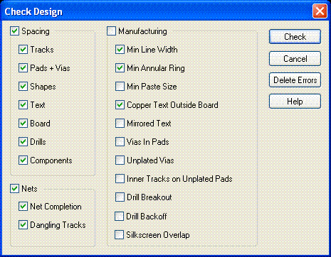
And here is part of the output generated:
Design Rule Check Report
 ------------------------
Report File : D:\My Documents\Roderick\Solar Bike\ptc (PCB - Design Rule Check Report).txt
 Report Written : Wednesday, October 21, 2015
 Project Path : D:\My Documents\Roderick\Solar Bike\ptc.prj
 Design Path : D:\My Documents\Roderick\Solar Bike\ptc.pcb
 Design Title :
 Created : 9/15/2015 11:07:07 AM
 Last Saved : 10/21/2015 4:33:11 PM
 Editing Time : 5204 min
 Units : thou (precision 0)
 Results
 =======
Component to Component error (Cm-Cm) at (10905 8747) on layer "[Top]".
 L12 - L1, Gap is 0.
 Component to Component error (Cm-Cm) at (9890 12353) on layer "[Top]".
 L1 - L6, Gap is 0.
 Component to Component error (Cm-Cm) at (8407 9740) on layer "[Top]".
 L1 - L2, Gap is 0.
 Component to Component error (Cm-Cm) at (9055 8747) on layer "[Top]".
 L1 - C1, Gap is 0.
 Component to Component error (Cm-Cm) at (9740 8747) on layer "[Top]".
 L1 - C2, Gap is 0.
 Component to Component error (Cm-Cm) at (11020 12309) on layer "[Bottom]".
 L7 - L1, Gap is 0.
 Component to Component error (Cm-Cm) at (8463 9760) on layer "[Bottom]".
 L1 - L2, Gap is 0.
 Gap in Net "LOGIC_GND" between (8025,8280) and (8025,8060)
 LOGIC_GND.
 Dangling Track from (8025,8060) to (7885,8060) on layer Top Copper
 Dangling Track from (7890,8414) to (7880,8420) on layer Top Copper
 Dangling Track from (8150,8420) to (8148,8415) on layer Top Copper
 Dangling Track from (8362,7455) to (8365,7455) on layer Bottom Copper
 Dangling Track from (10260,7595) to (10260,7600) on layer Bottom Copper
 Dangling Track from (10215,9215) to (10215,9220) on layer Bottom Copper
 Dangling Track from (9100,9305) to (9100,9298) on layer Top Copper
 Dangling Track from (8201,12365) to (8215,12365) on layer Top Copper
 Dangling Track from (8204,12875) to (8215,12875) on layer Top Copper
 Dangling Track from (12204,12245) to (12190,12245) on layer Top Copper
 Dangling Track from (13210,11384) to (13210,11345) on layer Top Copper
 Dangling Track from (12630,11345) to (12668,11384) on layer Top Copper
 Dangling Track from (12110,10580) to (12110,10591) on layer Top Copper
 Dangling Track from (8735,8580) to (8735,8580) on layer Top Copper
Number of errors found : 22
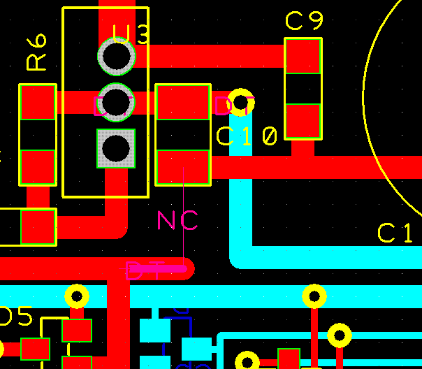
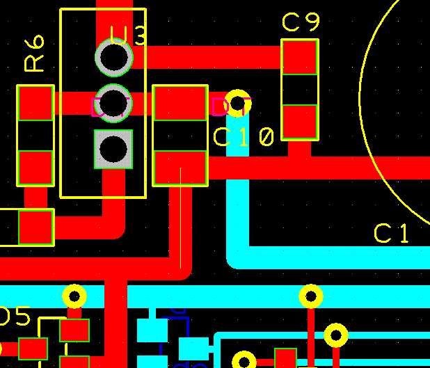
I love this part of the design, catching errors and weaknesses and fixing them. That was my career for over 30 years – fixing things. First I will look at the error in red above, the Gap in Net. It’s a real error, and I’m blogging in real time as I pursue it. so let’s look around coordinates (8025,8280).