I’m taking some time off from layout to check part footprints (aka land patterns).
Silly me, I thought earlier that checking the footprints would be a simple formality. When I worked at a corporation as an engineer, the CAD components were always made by someone else, usually with a footprint approved by Corporate Engineering. But in this hobby design, I’m finding that almost every footprint has some imperfection, and that when footprints are adjusted, the layout needs to be adjusted slightly, too.
Important note to self: Be sure to check all footprints BEFORE starting PCB layout.
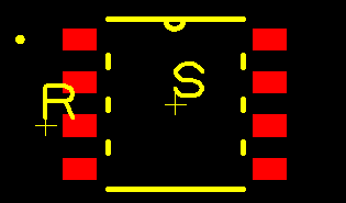
Below is one of the footprints that had a critical weakness.
While I was doing layout, I noticed that I was continually adjusting the 1206 footprint components by a few mils off the 5-mil layout grid. The default 1206 footprint in DesignSpark is two 63-mil square pads, with a center-to-center spacing of 134 mils. Possibly the part was translated from the metric, where 3.2 mm x 1.6 mm were the controlling dimensions. I adjusted this footprint to be two 70-mil square pads, spaced 140 mils center-to-center. This should make layout on the 5-mil grid much easier. I also adjusted the 1210 footprint in similar fashion. These changes threw off the existing routing for an awful lot of traces by a mil or two in various directions, and a lot of adjustment will be needed. I’m not going to fix up the layout just yet, because I’m still checking the footprints of the rest of components.
Update: I’ve been checking footprints every day, and am STILL not done. I’m editing footprints wherever possible to conform to a 5-mil grid, making pads larger as needed. This often impacts the layout for every instance of the modified part in the design. The changes are so extensive, that I feel more comfortable fixing up the layout after making each part change. If I waited until all the parts were changed, I’d be more likely to overlook something. Hopefully, just one more day of checking footprints.