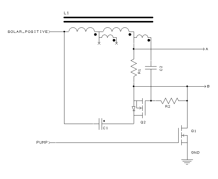
In the circuit above, an oscilloscope was connected across L1, with the SOLAR_POSITVE line used as a ground reference. The crude animation below shows the result.
To recap previous articles, during the “pump” phase, Q1 turns on for 20 µS, building up a current in L1. This is the -28 volt swing below ground. After that time, Q1 turns off, and the current continues flowing in L1, driving up the voltage into the positive region, and charging C1. The switching converter is operating in discontinuous mode – that is, current stops flowing in the inductor between pump cycles. There are a few overshoots and some ringing on the waveform – those will be snubbed out later.
The dimensions of the negative-going pump pulse are constant, but note that as C1 charges up, the height of the positive-going charge pulse gets higher, and the width gets narrower. This means a higher voltage, but shorter period of time. The minimum pulse width is about 12 µS, a figure that will be important in a moment.
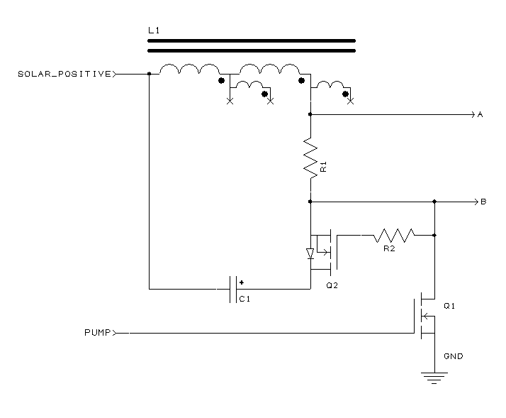
The first attempt to enable synchronous rectification was to connect an additional winding to drive the gate of Q2 as follows:
In the above, there were 14 turns of wire on the main inductor, and the inductor would be subject to voltages of between -28 and +40 volts. Since the MOSFET Q2 could only withstand ±20 volts on its gate, 6 turns were used for the gate winding, meaning that the theoretical voltage swing on the gate would be (-28*6/14 =) -12 volts to (40*6/14) = 17 volts.
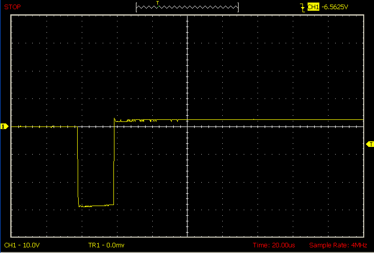
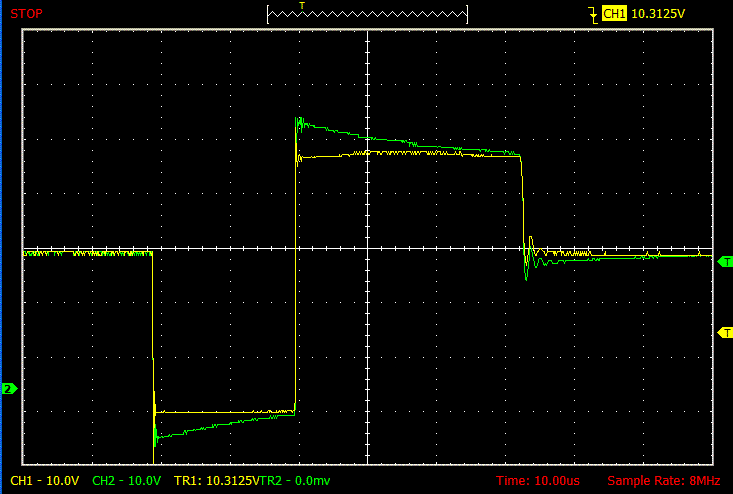
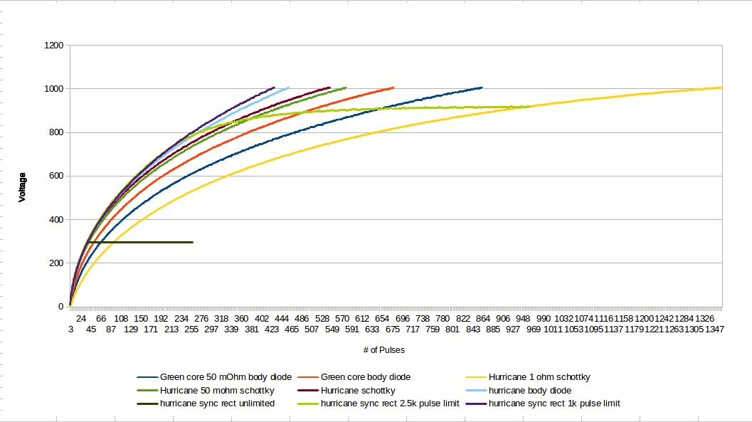
If Q2 was an ideal transistor, everything should have worked. However, the reality was that once this circuit was hooked up, the output voltage leveled off at a fairly low voltage (see the “hurricane sync rect unlimited” curve on the final graph). An oscilloscope trace showed the following:
In the most positive portions of the trace, the gate of Q2 (green) is about 4 volts higher than the source (yellow), which is just enough to start turning the transistor on. That’s what we want for synchronous rectification. Unfortunately, the world is not perfect, and even after the gate voltage goes negative, the transistor stays on for a while, conducting current back into L1, all the way down to the negative supply for perhaps 5 µS. When Q2 does manage to turn off, the current in L1 continues to flow, and the voltage zooms up to the most positive point again, turning on Q2 again. This is apparently a very efficient process, because the cycle repeats about 10 times without any additional energy input before finally dying out, presumably dissipating the energy on C1 deposited by the initial long pulse of charging.
I needed to have the gate drive for Q2 disappear about 5 µS earlier. There was no circuit that could activate off a future falling edge (that would violate causality), but what I could do is presume where that falling edge would be, and generate a gate drive that was 5 uS shorter. One way to do this would be digitally, generating a pulse to the gate of Q1 first, then a pulse of proper duration to the gate of Q2 just as the first pulse ended. Unfortunately, that would require level-shifting circuitry to generate high-side drive for Q2, and in the final implementation, there will be 12 Q2’s, each with a unique drive requirement. Too complicated.
If I could guarantee that the converter would operate in continuous mode, there would be other solutions, including putting a ferrite bead in series with Q2 to keep current flowing while the gate was forced down to a negative voltage by the next pump pulse. Unfortunately, I can’t make that guarantee in my design.
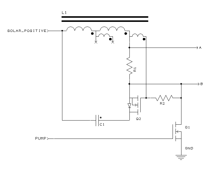
I finally chose the simple scheme below. It’s still self-timed, and should work regardless of whether the converter is in discontinuous or continuous mode.
I chose C2 to be 10 nF, several times total gate capacitance of Q2, since C2 and the gate form a capacitive divider during turn-on, and I wanted a good solid drive voltage at the gate. Because C2 would charge during the pump phase, and boost the voltage from the gate winding during the charge phase, the number of turns on that winding was reduced to 3. After setting the value for C2, and knowing the initial gate voltage at turn-on, it was a simple matter of using the RC decay formula to find a value for R2 that would lead to the voltage dropping below Vth 5 µS before the end of the charge pulse (this was where that 12 µS time from above came in. Details of the calculation are in my notes.) The calculated value for the resistor was 1.5 kΩ.
I put a small potentiometer in for R2, and started it at 2.5 kΩ, which corresponds to the trace labeled “hurricane sync rect 2.5k” below. With a value of 2.5 kΩ, the voltage went higher, but still hit a plateau. I finally decided that 1.0 kΩ would be the best working value for R2.
Note that these values of capacitance, resistance, and inductor turns are just for this breadboard, which contains a specific inductor for L1 and MOSFET for Q2. The final project undoubtedly be tweaked somewhat. Fortunately, if I need to adjust component values on the final PC board, a wide variety of values will fit on the same surface mount pads.
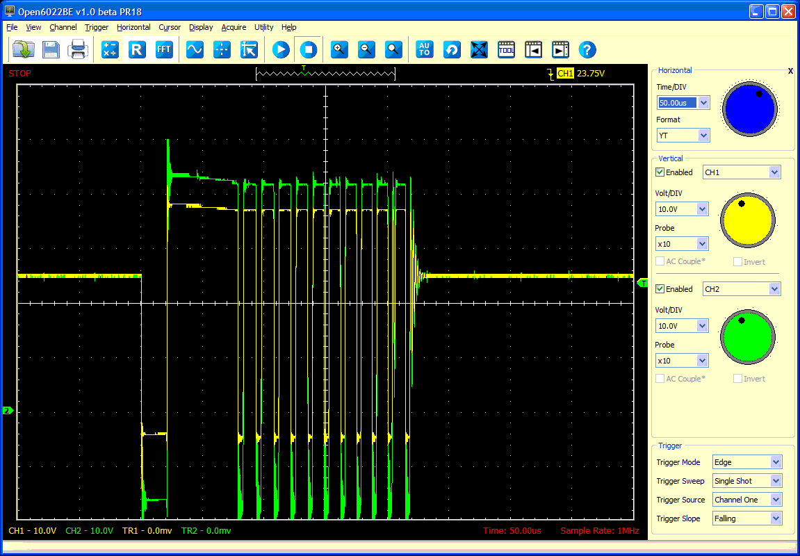
So it works!
Ideally, I would want to drive the gate of the synchronous rectifier hard until the last possible moment, then turn it off quickly. With the scheme above, the gate drive decays gradually, and Q2 is probably unsaturated (in the linear region) for some portion of the charge pulse. I can live with this because:
- The body diode will still carry current even if the transistor is only weakly conducting, or even off.
- There is still a noticeable gain in efficiency.
- I still get to claim bona fide synchronous rectification as a feature of the project.
A second issue is that the duration of the gate drive is fixed for a given output voltage, being most efficient at the highest voltages, where the gate drive has maximum duration, and the charge pulse has minimum duration. This is actually not so bad for a number of reasons:
- Lower output voltage is only encountered during start-up, not during normal operation. If there are batteries that aren’t completely dead, low voltage will never be encountered.
- The pump pulse width will be fixed in most cases. This means that the charge pulse width will be fixed in typical operation, too. To vary the amount of power delivered, the plan is to increase or decrease the number of pulses per second, not change the pulse width.
- The body diode will still carry current even if the transistor turns off early.
- There is still a noticeable gain in efficiency.