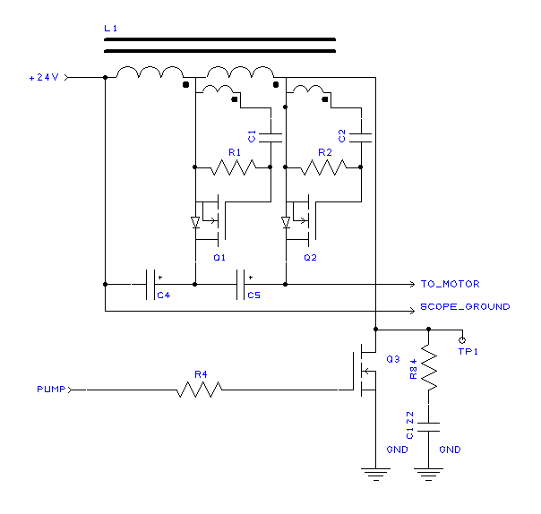
The core circuit for the Solar Bike’s power converter is conceptually shown above. A positive-going pulse goes into the PUMP input, turning on Q3 for a few microseconds. Current builds up in L1, reaching a peak of perhaps 40 Amps. When Q3 turns off, the voltage across L1 zooms up to whatever it takes to maintain the 40A current. This current passes through the body diodes of Q1 and Q2, charging capacitors C1 and C2. Extra windings on L1 generate a voltage on the gates of Q1 and Q2 at this time, turning them on briefly. In addition to making the charging of C1 and C2 a little more efficient, this also provides some voltage equalization.
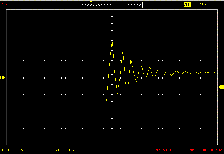
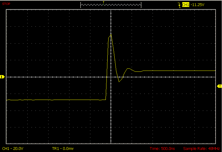
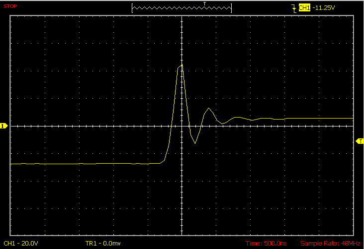
Engineering question: What voltage must Q3 withstand on its drain? The input voltage of +24V is a start, but since it comes from a solar panel, perhaps it could be as high as 40 volts. Added to that is the voltage stored on C1 and C2, the voltage used to drive the motor. Let’s say that the motor voltage is 30 volts absolute maximum. 40 + 30 = 70, so a beginning designer might think that a MOSFET rated 70 volts Vds would be enough – perhaps 80 or 100 volts to provide a safety margin. But hold on a minute. Take a look at the real-life waveform on the drain of Q3 below.
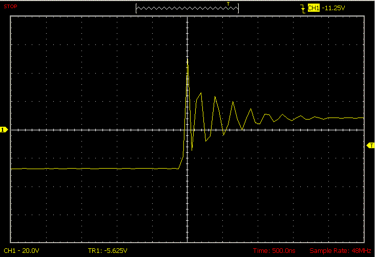
In a perfect world, when the PUMP pulse goes away, the voltage would clamp at 24 volts plus the output voltage across C1+C2, but in reality, it overshoots and rings. In anticipation of this happening, I put the following pad patterns down for R84 and C122:
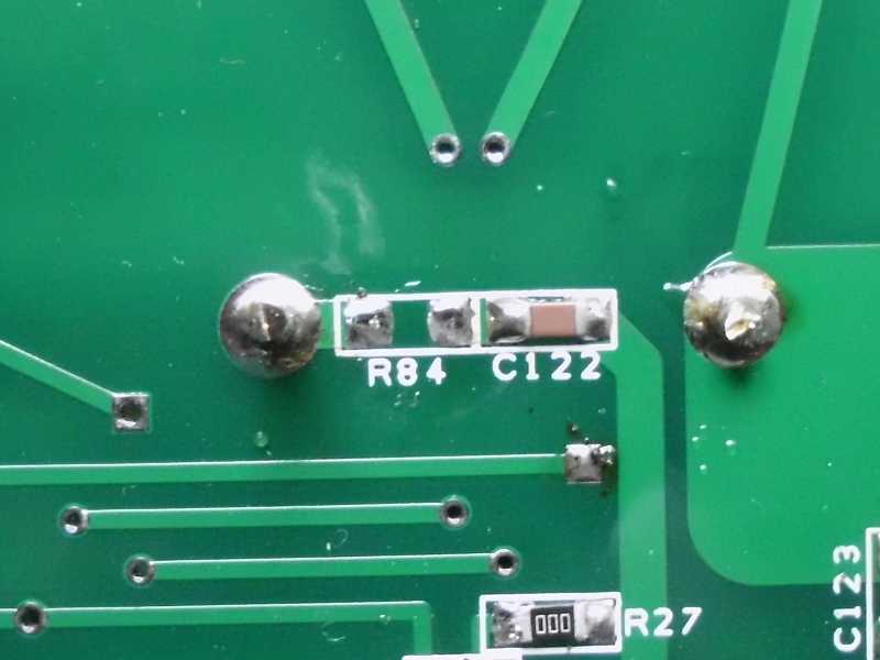
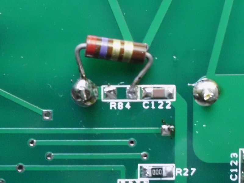
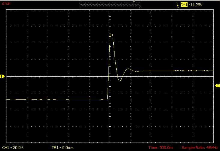
The idea of an RC snubber is to absorb and dampen the ringing. But what value of components should be used? We can see the resonant frequency (about 4.5 MHz) of the ringing from the previous trace, but we need to know the individual L and C in the circuit, in order to match impedances at that frequency. To figure that out, a zero-ohm jumper was installed for R84, and 10 nF (0.01 uF) was installed as C122.
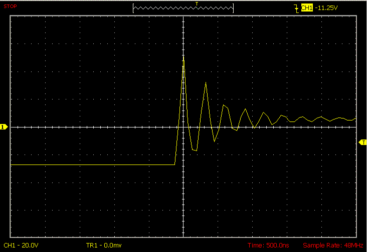
As expected, the frequency of the ringing is lowered from the original 4.5 Mhz, to about 3.6 MHz. Using the basic engineering formula of

we can determine that the equivalent original capacitance is 16 nF, and using

that its impedance at the original ring frequency was 2.2 Ω. The details of the calculations are in my handwritten notes.
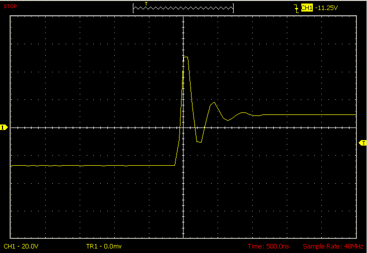
Again, skipping over theoretical details, this means that we would want C122 and R84 to be in that ballpark. I didn’t have those exact values on hand in 1206 surface-mount size, so I used a 10 nF, 50V capacitor, and a 2.7 Ω resistor. I put a few pulses through the circuit, and took the following trace:
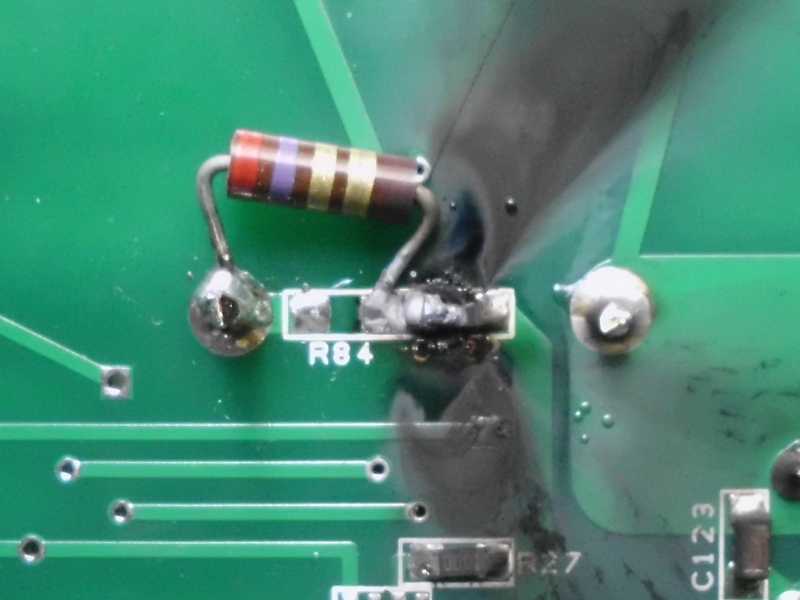
The snubber acted like it wasn’t even there. Turned out, it wasn’t! I measured the 2.7 ohm resistor, and found it to be open. Apparently, the supposed 1/4 watt film resistor couldn’t handle the surge current and blew out. Learning: this must be why in some switching applications, manufacturers specify that resistors must be carbon composition. I replaced the blown resistor with an old-style 1/2 watt carbon composition resistor:
But when power was applied to the circuit, there was an incandescent glow on the board.
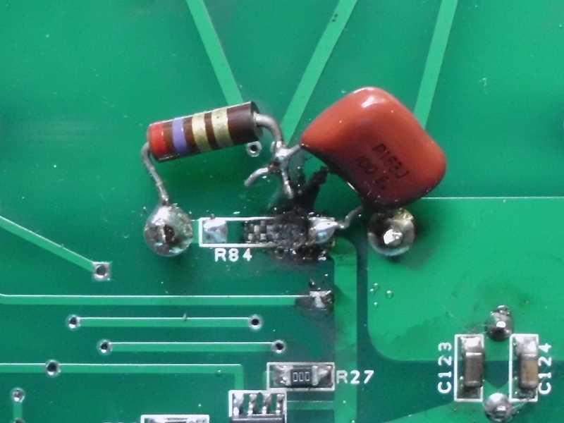
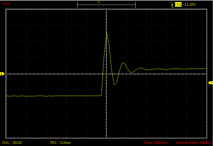
I remembered something that an analog CRT sweep designer (I think his name was Rick) told me in 1981, at my first permanent job. He said that those snubber resistors get hot. I didn’t think too much about it at the time, but the memory resurfaced after this incident. My next try was with a 2.7 ohm resistor, and a 16 nF mylar capacitor rated for 100 volts.
In an ideal world, I should have been able to move the snubber from being across the drain and source of Q1, and put it across L1, instead. In theory, those points should be the same for AC purposes. And that would mean that the capacitor voltage would swing from -24 volts to +75 volts, instead of from 0 to 99 volts. That would mean less stress on the capacitor, as the peak voltage across it would be lower. So I tried it.
The overshoot voltage was actually worse with the snubber across L1. Lesson: if the snubber is supposed to protect a transistor (Q1 in this case) from overvolage, put the snubber as close to the transistor as possible. To put it elsewhere is like having a guard dog in a house a block away, and expecting it to watch your back yard.
Up until now, we have been ignoring R4, the gate resistor of Q1. Originally, this was 2 ohms. When designing, I put in a resistor because every design I’ve seen puts one in. As a novice designer, I thought that the faster I could drive the transistor, the more efficient it would be. But I had neglected the overshoot that occurs when a waveform switches too fast. I’m beginning to see why a gate resistor is important.
To be safe, I’m going to increase the voltage ratings of both Q1 and the snubber capacitor.
My next investigation will be into what destroyed Q2 in a previous experiment. My hunch is that it was overvoltage on the gate.