The previous experiment in the field left many questions that would best be answered on a lab bench, where better instrumentation was available.
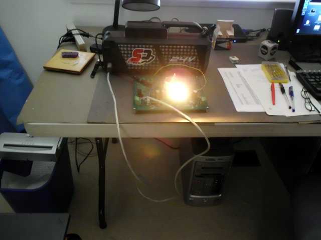
I fired up the same test as the previous day, a sweep of decreasing switching periods that was intended to find a maximum power point on the solar panel. I did not expect to actually find a max power point from a set of batteries, though. My test theoretically pulled 250W at the most, and I know from experience that the battery bank is capable of 750W. But I hoped to examine waveforms on the board.
The test is scary to watch, especially indoors. There is a whine from the inductor that gets higher and higher in pitch. The lamp gets brighter and brighter, like a warp core getting ready to explode. When it’s lighting up the room, and it looks like it can’t possibly get any brighter, it goes one step brighter. And then…

There was a bright flash, and arcing sound, and the smell of burned vinyl. The lamp went out. I cut the power immediately. Okay, here we go again. Burns are part and parcel of designing switching power converters. Did the main switch burn? Surprisingly, no. I cautiously touched its heat sink. Barely warm. Did the PICAXE burn? After scrutinizing the board a bit more, I noticed something odd in one area. It wasn’t immediately obvious, because it was initially obscured by a large connector and heat sink.
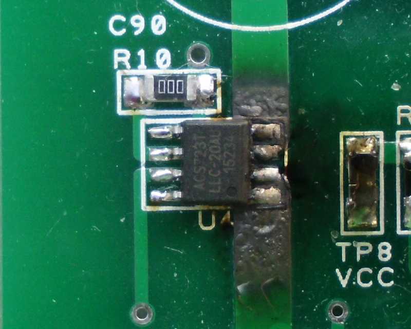
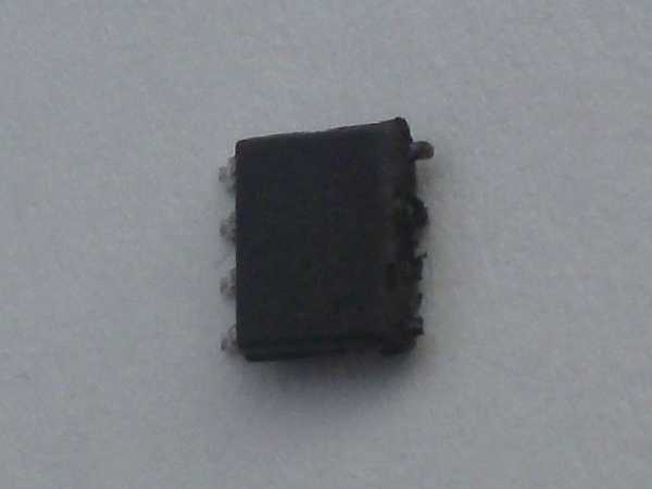
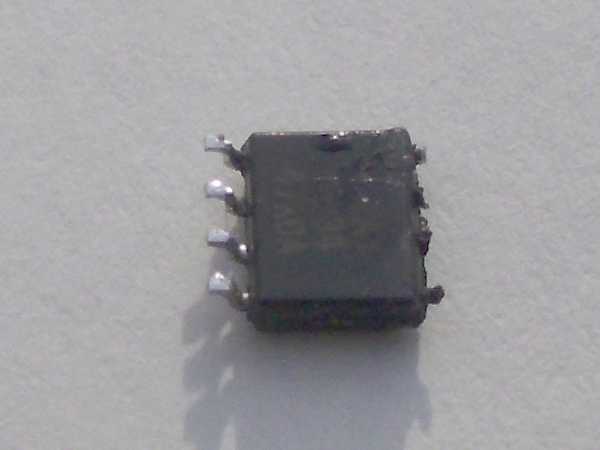
According to the last data sample captured just before the burn, the current flowing into the input was 6.8 amps. That shouldn’t have been a problem for the part, which was designed to measure 20 amps, and withstand even more. Could it be that I had a defective part? Or that these parts have some other basic problem? I checked the two other instances of this part on the board. The other parts were rated to measure 40 amps, but even so, I had to believe that they still used the same metal leadframe to carry the current, and that the only differences were in the amplification factor of the silicon.
The sister parts looked fine. In fact, the soldering was messier on those than on the U4 that burned. And according to the telemetry log, U6 was carrying even more current than U4 when the incident occurred. The next move was to use hot air to carefully remove the failed part.
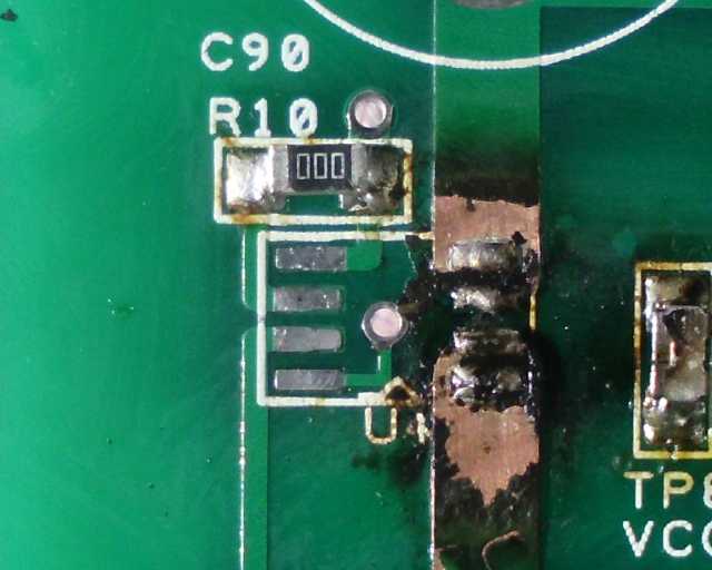
Given this data, the root cause seems to have been bad soldering, or put another way, my fault. I may have used solder wick to clean up the appearance of the pins on U4, while leaving the other two parts messy. This could have led to a poor contact between the current-carrying pins on the chip, and the traces. If there was intermittent contact, it could have drawn an electric arc. Even a contact resistance of 100 milliohms would have dissipated 10 watts at 10 amps, more than enough to heat the tiny contact area. If I had to guess, I would say that the initial heating was mainly under the pins on the bottom right, since that trace delaminated, and the top one did not.
My takeaway for the future is to put a lot of solder on the current-carrying pins of these chips, and further, I will put a drop of liquid flux on the area, and anneal the solder with a hot air wand.
So the land pattern for this chip is burned on the board. I can’t put a new chip in place there (at least, not easily) because the pins of the original chip are still welded to the trace. I could just run a jumper across where the chip used to be, and forget input current monitoring. Maybe I’ll do that, at least initially, to see whether the PICAXE is still alive.
I could try to grind down the pins that are welded to the trace, then solder a new part in place. Nothing to lose – if I destroy the trace, I’ve destroyed something which is unusable, anyway. I could also run heavy wires to the chip, in lieu of the traces. This might be step two.
Another possibility is to use the prototype area on the board. I have a spare land pattern for an SO-8 package there. I’d still have to run heavy wires from the chip.
UPDATE (24-FEB-2016): I haven’t been able to work with the board much, due to other commitments. I changed the main MOSFET switch, and jumpered power to bypass the current sensor. The new switch burned out instantly. I then found out that the MOSFET used as a synchronous rectifier had burned out, too – fused into a low-resistance lump between all leads. I now believe that overvoltage on the gate of that part caused the failure. Once the synchronous rectifier failed, it took the main switch with it. Once the main switch was fused into a lump, virtually unbounded current could flow through it, which is probably what burned out the ACS723.
UPDATE: (05-APR-2016): Later experiments suggest that overvoltage on the drain of the main switch was the culprit. But the synchronous rectifier may still have failed from overvoltage on the gate; that must still be investigated.