For a long time, I had been unnecessarily avoiding transformers. I had been brought up at the dawn of the digital era when we used capacitors for things if at all possible, not inductors.
The advantages of a transformer-centered equalization scheme became too powerful to ignore, though, so I finally decided to wind the custom transformer/inductor that was required. The previous scheme using a voltage limiter across each supercapacitor was imprecise and inefficient by comparison.
The new circuit will intrinsically charge each capacitor to an equal voltage, without op-amps as control circuits. If any capacitor is lower in voltage than the rest, it will automatically hog the lion’s share of the current from the transformer until that cap comes into line with the others. It will not matter if some capacitors have higher or lower values, or different leakage rates – the voltages will still be equalized, through the basic physics of loops of conductor in a shared magnetic field.
If I was going to wind my own inductor anyway, it would be easy to come up with the high-side drive voltage necessary to do synchronous rectification – just be one more wire per winding – so I’m going to do that, too.
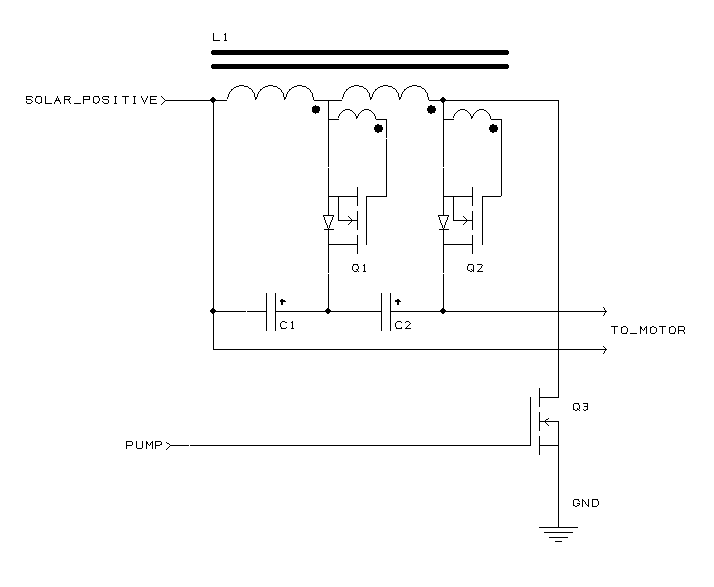
In the above diagram, L1 is the toroidal inductor. The actual part has 13 terminals, but only 3 are shown for ease of illustration. The wire labeled SOLAR_POSITIVE is coming from the solar panel, and has, let’s say, 24 volts on it. When we begin, let’s further assume that no currents are flowing anywhere in the circuit, and all capacitors are completely discharged. The PUMP signal is low, so enhancement mode N-channel MOSFET Q3 is off. Q1 and Q2, also enhancement mode transistors, are also off, as a transformer winding effectively shorts their gates to their sources.
At the start of the cycle (I call it the “pump” phase), the PUMP signal goes high, turning on Q3. A current begins to build up in the main windings of L1, as 24 volts is now being applied across the inductor. The small windings immediately have negative voltages across them, which is applied to the gates of Q1 and Q2. Since the transistors are already off, nothing happens.
After a few microseconds, when a sizable current has built up in L1, PUMP goes low, turning Q1 off. (I call this the “charge” phase.) The current in L1 cannot instantaneously vanish, so it flows through the body diodes in Q1 and Q2, charging capacitors C1 and C2. A small positive voltage also develops across the gate winding of each transistor, but at during the initial charge cycles, this voltage is not high enough to turn the transistors on.
After some additional microseconds (or milliseconds, possibly), PUMP goes high, starting the cycle all over again. The PUMP signal pulses thousands of times per second, building up the voltage across the C1 and C2 to the desired level. The series combination of C1 and C2 provides the voltage that powers the motor.
To understand how the synchronous rectification works, consider C1, Q1, and the associated windings on L1 (the main winding which charges the capacitor, and the gate winding going to the gate of the transistor). The voltage across the gate winding is in fixed ratio to the voltage across the main winding, by basic transformer rules. The inductor is constructed such that once the main winding that is charging C1 attains about half the normal operating voltage, the corresponding gate winding has enough positive voltage to turn on Q1.
Why go through the trouble? Isn’t the body diode of Q1 already conducting? In fact, it is, but every real-world diode has a voltage drop across it. In many applications, we simply ignore this voltage drop, but if the diode has, say, 10 amps flowing through it, and the voltage drop is 1 volt, 10 watts are actually being dissipated (wasted) in the diode. If we can turn the transistor on to a very low-resistance state, we might be able to get that voltage drop down to 0.1 volt. That brings the power dissipation down to a mere 1 watt, making the enitre power conversion more efficient, and obviating the need for a big heat sink on Q1.
Review from previous blog entries: Why use a stack of capacitors in series, instead of just one capacitor rated at a high voltage? Answer: Unfortunately, with present technology, supercapacitors are limited to a 2.5 or 2.7 volt operating voltage, best case. I would love to use a single 8-farad, 30-volt capacitor, but it doesn’t exist today. [Aside to inventors: if you invent something with supercapacitor density, that will tolerate 100 volts, you will change the world.]
Review from previous blog entries: Why not charge the whole stack of capacitors just at the ends, rather than this convoluted scheme involving so many inductor windings and transistors? Answer: since the supercapacitors will be running near their maximum operating voltage, the best way I can think of at the moment to keep any given capacitor from exceeding its operating voltage is to make sure that the voltages across all capacitors are substantially the same. Then, I can simply monitor the voltage across the entire string, and stop charging if the voltage is about to exceed safe levels.