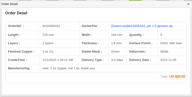
At this time (Nov 8, 2015), I’m waiting for blank PC Boards to come back. The process is certainly different from when I was in High School some 40 years ago. In those days, I would create physical artwork on Mylar by using rub-ons and tape. I would then have to take that to a photo lab to be reversed into a negative. From there it was an arduous process of spraying photo-resist on a board, exposing it, and etching it. Once I had a big board to etch, so just walked into a PCB shop and paid them to etch it. It would have been scary to send actual artwork from Hawaii to the continental US for fabrication, because what if they lost it? (Not to mention, I couldn’t afford it.)
Even decades later, at work we still had to send out a physical Gerber tape, as there was no internet. And there would still be a lot of back-and-forth on the phone with the fabricators about anything that was strange or difficult. At least we had tools to do schematic-to-PCB checking, and some design rules.
Fast forward to the present. Though we used to pay a whole department of people to oversee the PCB process – today, it is trivial. All the design was done on my $80 computer at home. Schematic matching and Design Rule Checking were automatic. No point in making a board at home, anymore, as I have money, and there are literally dozens of places on the internet that make boards. As the process is highly standardized and automated now, I have no fear of contracting the job out to the place with the lowest price, even if that isn’t nearby.
Ultimately, I chose a place in China called pcbway.com . I had seen reviews of their product that showed low-quality silkscreening in some cases, poor alignment, and flaky communication. Further, they openly paid people for positive reviews (it’s offered on their website). However, I was able to rationalize myself out of the potential problems. The messed up silkscreen was in a case of someone ordering black ink on a white solder mask. I had everything very conservative and proven in my design. Regular green FR4 substrate. White silkscreen, green solder mask. 10/10 mil minimum trace/space. Only normal-sized through vias. I even had tooling holes in the corners of the board, although I suspected that they would neither need nor use them. The only unusual thing on the board is 2 oz copper, but even that isn’t so weird.
Before submitting the order, I asked a question on their contact form. It was about drill backoff errors in my design. I had pads that were smaller than the attached traces in some cases, which might have led to issues in the old days, when a manufacturer might edit the Gerbers to back traces off the center of the pads, leaving a visual target for someone to manually drill. After a day, a woman sent an email saying that it was a problem, and that I should fix the error, or she could have someone help me with it. After reading and re-reading her response, I decided that she hadn’t really understood the question or the issue, and just picked up on the word, “error.” After consulting with various people on the internet, I decided that these were not real errors, and proceeded to submit the order.
For 5 boards, I’m paying $122 including shipping (by redeeming the $5 new-customer coupon.) That’s less than 36¢ per square inch, for a prototype run. Other Chinese vendors were in the sub-$200 range, but elsewhere in the world (including the USA), prices were two to eight times as much.
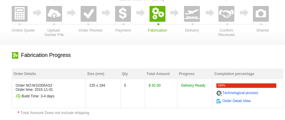
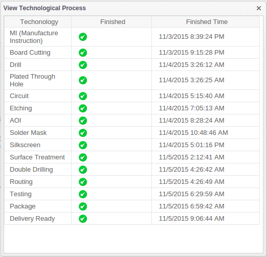
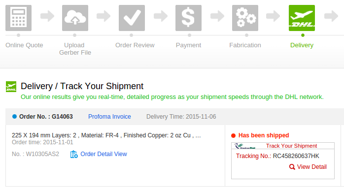
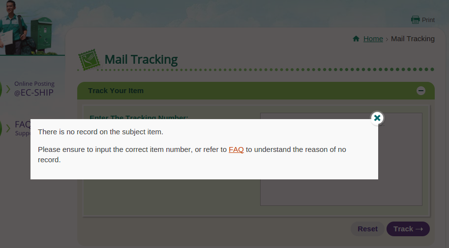
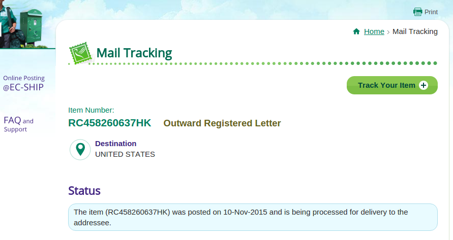


UPDATE, 16-NOV-2015 8:50 AM: The package just arrived, signature required. That made the turnaround time from file upload, to package on my doorstep, 17 days, or 14 days from Paypal payment. I wasn’t expecting the boards for another 2 weeks, since I elected HK Post shipping rather than DSL. There are still components enroute from Mouser. In curiosity, I went back to the HK Post tracking site to see the status of my package. The site now once again says it has no record of the package.
UPDATE, 18-NOV-2015: Yesterday, I opened the package and took a look at the boards. Posted a review of pcbway here.