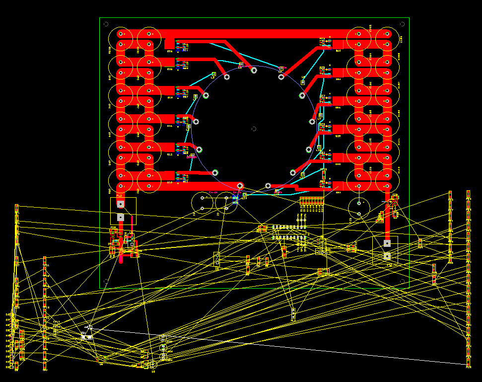
Around September 15, 2015, I felt confident enough in the design to start printed circuit layout. I’m using a free tool called DesignSpark. This is how far I got as of September 29, 2015:

Although I don’t work on this layout every day, I do put many hours into it. So far, I think I’m averaging about 10 minutes to place and route each component. This might seem to be low productivity to someone unfamiliar with layout, but considering multiple re-do’s over the course of layout, I think it’s not bad. Remember that in a large software project, good productivity is one line of code per day, per person.
My strategy for layout was first to place the main inductor at the middle of the board, then place the supercapacitors and synchronous rectifiers. I tried to use traces as thick as possible, and will route high current paths on both sides of the board when possible. I also need to add copper fills to some areas, because the PCB copper is the only heat sink that the synchronous rectifiers will have.
Next after that, I put in the input and output connectors, bulk capacitors, and current sensors, since these are to be near the edge of the board, and the wires need clearance.
The next most critical thing is the main switch (MOSFET), which must be in a location that can be well heat-sinked, as well as physically close to the load it will drive.
Oddly, the lowest priority for routing is the processor, which is low power, anyway, and can go pretty much anywhere.